My output board had a few flaws, one of which is that it includes level shifters for an I2C bus operating at 5V but the fpga is operating at 3.3V. I need to bypass the level shifters. Also, the output board has the normally open link connected to the normally closed switch line in its 'idle' or unactivated state, but this should be reversed so that NC link is hooked to the NC switch line and the NO link hooked to the NO switch line unless the relay activates to flip these connections.
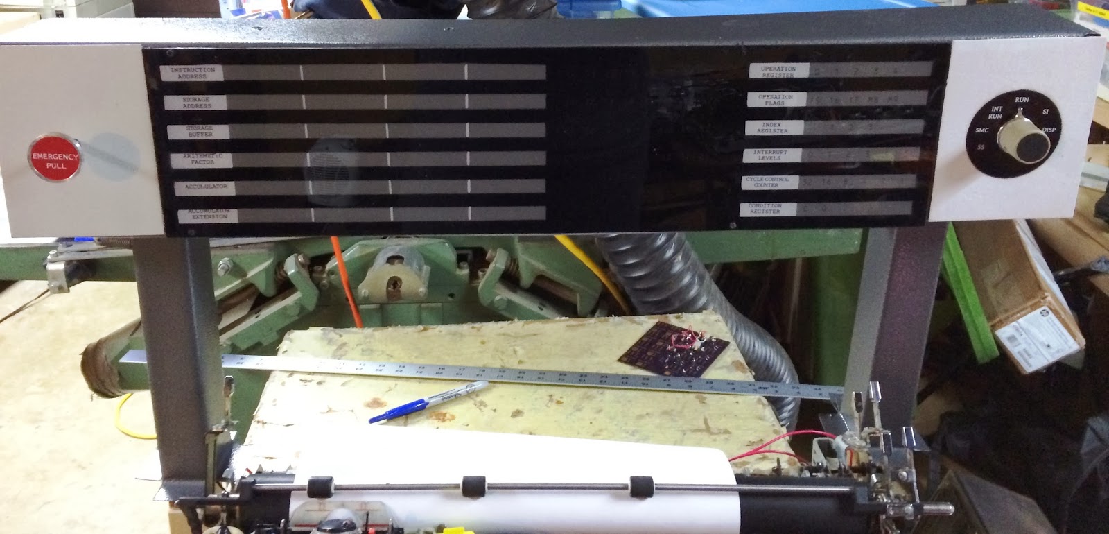
 |
| Interface testing from rear of Documation reader |
I made the changes to the output board to fix the defects I discovered. It is now working just as expected, although the reader doesn't recognize that the reset button is released when my cable is attached from the output board. I have to dig into this. It could just be excessive resistance due to the log wire runs, two connectors and relay contacts. If that is the cause I can relocate the relay much closer to the machine or inside the card cage.
The card reader starts up with FEED CHECK and ATTENTION illuminated, but doesn't reset when I press NPRO. I did a bit of debugging of the adapter logic plus the IBM interface logic for the 2501. The ATTENTION light is an error, it should never be lit because the two conditions that cause it, open cover and stacker full, are both always false in my implementation.
 |
| Storage scope to diagnose analog condition of aperiodic signals |
 |
| Bus pirate to test serial protocols and snoop on lines |
Now I am entering into the serious debugging phase of my adapter logic as well as the implementation of the 2501 reader interface logic in the 1130. I will take some time to determine what signals and states should be displayed on the eight LEDs and output on the 14 diagnostic lines for use by the hardware monitor. In addition, I put in an hour carefully comparing the ALD pages for the IBM logic for the 2501 interface to my implementation. I found a few errors and corrected them. In some cases I had two spellings for a signal, so that the proper signal wasn't brought to the gates that needed it.
I learned more detail about how the 2501 works, which my model of its behavior didn't match. For example, any time the motor is running if any photocell is blocked at FeedCB2 time, a feed check is detected. This is the cause of my current symptom. I altered the logic to make these all report light detection except when reading card columns.
Due to blurry photos of the ALD pages, I used an inverted hopper empty signal in one module when I should have used the normal version - this caused spurious feed check conditions. I kept hammering through the logic and the testing, almost all caused by subtleties in the timing of the 2501 mechanisms which were not perfectly reproduced by my emulation logic. By Monday evening, the issues with the Feed Check and Attention conditions were resolved and I could move into core function testing.
 |
| Reader at startup with Feed Check that mimics 2501, but resets with NPRO button |
14 of the input signals from card reader were connected to diagnostic output ports on my fpga board to allow me to hook up the logic analyzer and monitor the correct behavior reading cards. The reader will be in 'local' mode where it reads continuously whenever it is made ready. I will also monitor the reporting of the error conditions so that I am sure of the relative timing and behavior of the reader.
I have the adapter working to the point where it clears the initial 2501 feed check and then does a feed cycle to become ready. This means that the adapter logic is correctly setting up the prefeed station card lever. However, it didn't activate a read by the Documation.
Further, when I introduce a hopper check error, it doesn't drop the 2501 out of ready state.This is likely because I am not yet reflecting the Documation errors into the emulated 2501 machine so it never happened as far as the 1130 logic is concerned. In spite of that, I am clearly making progress on the adapter and interface logic as well as my emulation of the 2501 mechanism.
When I watched with the hardware monitor, it was obvious that my serial link is not fast enough to reliably pick up the 6 microsecond duration index marker. I can tighten it up a bit by stripping out some inefficiency in the polling routine, such as transferring unnecessary words for the second and third chips as those two use only one of the two 8 bit banks for signals.
That improvement would give me a sample about every 200 microseconds and the bits of card column may differ (being spread across two banks) by no more than 60 microseconds). Since the data is valid for a guaranteed time of 864 microseconds from the index marker rising edge, this is fast enough to pick up the card columns. However, it is NOT fast enough to reliably see a 6 microsecond index marker pulse.
I need some registering hardware in the interface electronics, ahead of the MCP23017 chip, that will latch in the photocell values when the index marker edge falls, and hold them until the next rising edge of IM. This is a D transparent latch with the index marker acting as an transparency enabling signal. I need a small board that provides this functionality and can be included inside the aluminum inputs interface case.j
I need some means of knowing that an IM occurred in the interval since my last poll. The MCP23017 chip gives me the means to do this by way of its interrupt capability. I can configure the chip that receives the IM signal to make that one pin enabled for generating interrupts. When the pin is different from the default value I set for it ('0'or off), e.g. whenever an IM pulse occurs, the chip will register an interrupt which is reset when the values of the bank are read via my poll.
The interrupt bit is not cleared until the last of the bits from the bank that generated it have been read. This allows me to put the interrupt bit (new IM since last poll) into the same bank as I normally read, alongside the IM pin. The 'real' IM signal will be ignored generally, but will serve to trigger the interrupt which generagtes my 'IM had occurred since last read' bit which I do use. The race condition that we can reset the IM interrupt in the midst of the 6us pulse, thus receiving an interrupt on the next round in error, can be managed by ignoring two IM updates in a row in the polling routing.
I don't think I explained this clearly but the changes are fairly simple to the existing input board: routing the READY signal to another bank to make room for the IM interrupt occured bit and routing the interrupt pin alongside of the IM signal on its bank. Some additional initialization writes to configure the chip will complete the change. Of course, I have to put the board with the 12 D latches in series with the 12 row signals going to the input board to hold the card values.
 |
| PCB to latch the 12 card row signals between IM pulses |
The design is done, with the PCB manufactured tonight. I have all the latches and other parts on hand, thus it will require only about 15 minutes of drilling holes and another 15 minutes of soldering will yield the completed board ready for testing.
 |
| Circuit board ready for drilling, component installation and testing |
 |
| Components installed, ready to install in inputs box |
Once those were soldered into place, I rerouted the 'ready' signal from the second chip to an unused pin on the first chip, freeing up a pin I can use to detect the interrupt that is set whenever the IM pulse is detected. Hooking into the interrupt pin on the chip was the most challenging part of the change, since my input board design did not use those pins and consequently didn't route them anywhere. I had to tack a wire onto pin 20 of a SOIC sized surface mount chip whose pins are a mere 1.4 x .4 mm (.05" x .015") in area.
I am doing a major rewrite of the logic for driving the MCP23017 chips for the card reader serial link, because I had to make quite a few changes to tighten up the timing and add the new IM detection method. The old logic handled each of the individual steps - e.g. write the address of a register, write the value of the register -- and for each it has steps to verify the request was taken and to wait for completion. It was cumbersome to read and hard to change.
The new approach introduces a transaction level module, where I can make a single request such as 'put these values at registers beginning at number xx', with the calls to this module easier to understand. There is a fair amount of changed code in the adapter module plus the introduction of this new module, which is chewing up a bit of time coding and synthesizing.
The testing showed that my wire soldered to the teeny pin of the MCP chip is bridging to the reset pin, keeping the chip in reset mode so the board doesnt work properly. I have attempted to place this wire on the chip at least ten times already and had to flail away at it again until I got the wire attached without shorting the reset lead on one side or the signal input lead on the other side. I can now work my way through the
issues until I have the link working well again.
Unfortunately, when you make multiple changes at the same time, some electrical, some in hardware logic, some in the 2501 emulation strategy, some in the Documation driver strategy and some in testing approach, it can take quite a while to sort out where the sometimes tiny error exists that keeps things from working properly.
DISPLAY PEDESTAL COMPLETION
I cleaned up the rear of the two side plates - mode switch and emergency pull switch - then used JB Weld to bond nuts onto the back of the plates. These will be used to affix the plates to L brackets and those will be mounted inside the pedestal enclosure box to secure the plates in location. I have had epoxy fail repeatedly for holding nuts to the plate, but hopefully this product which is designed for metal to metal bonding will create a more dependable joining.
I need to have secure mounting for the side plates in order to validate the right locations for drilling the holes in the enclosure front flanges to pass the acrylic 'pins' of the plexiglass front panel. I will need a day for the nuts on the side plates to become solidly attached, the rest of the work on the pedestal must wait for this critical path item.
 |
| Pins attached to rear of plexiglass panel |
I have carefully measured the pin locations on the plexiglass panel and marked up the enclosure front flanges. The holes were drilled and the panel is ready to affix. I seated it in place and have to put on the anchors, which are axle stops, tomorrow.
 |
| Panel in place but not yet anchored. |
I picked up some Weld On #16 acrylic cement which is thicker and should fill gaps. I will give it 24 hours then test the security of the pins and hopefully move on to attaching the panel onto the enclosure. When it is in place, after I place an orange filter behind the panel, I can fasten the internal light panel in place and begin closing up the pedestal enclosure.
One of the pins popped off - it might have been the one of the original four that hadn't come loose and thus wasn't reglued. In any case, I glued it with Weld On 16 while the panel sits in place secured by two of the other pins. The top right pin seems a bit large in diameter to comfortably slide the axle stop over, and out of caution I used a cable tie for this top pin rather than risking breaking it off. Overall, the panel is now attached.
The circuit board is attached to a more complex bracket that is also hooked through holes in the bottom of the enclosure, forming a metal tab that extends horizontally and to which the rubber bumpers on the back of the circuit board can sit. It is fastened down with a twist tie around the circuit board and the metal tab. With the board held in place, the cables from the light panel assembly are plugged into position. A bit of foam rubber between the circuit board and the rear cover of the enclosure will keep the cables from working loose.
To help hold the pedestal up on the frame and to protect it before it is in place on the machine frame, I installed wood posts inside the metal stands of the pedestal. These are temporarily affixed to a wide base to keep the pedestal safely upright, but the bases will be detached and the wood posts connected to the frame when I am ready for that step.
After my amber/orange filter material arrived this weekend I put it in place, put the axle stop on the re-glued pin and anchored the last pin with the cable tie. In replacing the inner light panel into the enclosure, I encountered a number of fiddly and tedious fit and clearance issues, such as needing to notch away some acrylic spacer on the light panel to allow the pin fastener from the plexi panel to clear, trying to swing the assembly into the box with almost zero clearance at its 45 degree insertion angle, and screwing it into place.
Once that is done, I will move the inner light panel into position, secure it into the box and dress all the cables and rear circuit board. However,this process went badly. A pin snapped off the plexi panel, the inner light panel broke apart a bit, and a guidance peg inside the enclosure came off.
I am not even sure of the condition of the light panel, but every step forward I attempt to take is yielding further damage to the project. I had to walk away and will go back to this part of the project on another day. I am demoralized as the entire light pedestal portion of the project has been quite a frustration and far more problem ridden than there is any reason to expect.
DOCUMATION READER MODIFICATION
I will bring the stacker full switch signal out through the same DB9 connector as the stop and reset switch remote activation signals, allowing me to raise the 2501 Attention condition and light the Attention lamp based on this condition. I will also rewire the reset logic, placing a small relay inside the card cage to minimize wire length and cumulative resistance compared to the relay mounted on the outputs board in my current implementation.
I will only need one line to activate remote stop, one line to activate the remote reset relay, one line for ground and one line for the stacker full signal, while the existing cable carries five wires. A bit of rewiring of the DB9 connector is necessary and now the dummy plug is not needed to allow standalone Documation reader operation. The stacker full signal has to be routed through the debouncer miniboard inside the outputs box and then out to the inputs box for delivery on an unused input channel.
The small board to handle cards with an upper diagonal notch on the right side has passed its functionality tests, but I will put it aside until I am comfortable with the correct operation of the Documation reader in its unmodified state.
 |
| Quick daughter card to test the modification for Documation to read right-side notched cards |
XILINX WARNING MESSAGE REDUCTION COMMENTS
The conditional generation capability of the Xilinx toolkit is terrible. It will report errors in code that is inside a 'generate' block whose condition is false, thus it should be ignored. I will get the results I want only by leveraging an external C/C++ preprocessor to handle conditional code manipulation, even though that adds steps and opens some risk of code regression if I forget to make changes to the master code file.
The toolkit can be quite finicky over code that is working fine and widely distributed on the net - I find myself jumping through hoops to try to eliminate the warning message, but every extraneous, spurious warning is more noise that hides real issues.
One alternative solution to the warning message blizzard is to set up a script that will strip out all errors that are entered into a file of known false warnings, so that the synthesis report gets piped through this to yield high importance or new warning messages.
For now, I will put this effort on hold as it would introduce even more changes into a project while I am trying to debug it and achieve correct operation. Some changes are certain to go wrong and inject new errors that must be tracked and fixed.
No comments:
Post a Comment